Logic Gates: The Foundation of Digital Electronics
Logic gates are transistor circuits that implement Boolean operations on digital signals. They are the building blocks of adders, registers, multiplexers, memory, processors, microcontrollers, and FPGAs.
Learning Objectives
By the end of this lesson, you should be able to read truth tables for basic gates, write Boolean expressions, explain universal gates, connect logic gates to real voltage levels, and avoid common hardware mistakes such as floating inputs and overloaded outputs.
Digital Levels
Digital circuits treat voltage ranges as logic states, not perfect mathematical values.
LOWmeans a voltage below the input-low threshold.HIGHmeans a voltage above the input-high threshold.- The invalid region between thresholds should be avoided.
- Common logic families include 5 V TTL/CMOS, 3.3 V CMOS, 1.8 V logic, and lower core voltages inside ICs.
Always check datasheet thresholds before connecting different devices.
Basic Gates
AND Gate
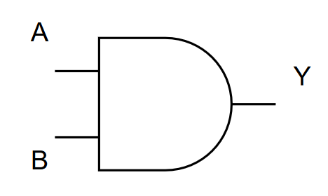
The output is HIGH only when all inputs are HIGH.
| A | B | Y |
|---|---|---|
| 0 | 0 | 0 |
| 0 | 1 | 0 |
| 1 | 0 | 0 |
| 1 | 1 | 1 |
$$
Y=A\cdot B
$$
OR Gate
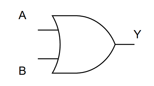
The output is HIGH when any input is HIGH.
| A | B | Y |
|---|---|---|
| 0 | 0 | 0 |
| 0 | 1 | 1 |
| 1 | 0 | 1 |
| 1 | 1 | 1 |
$$
Y=A+B
$$
NOT Gate
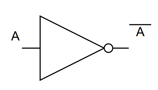
The output is the inverse of the input.
| A | Y |
|---|---|
| 0 | 1 |
| 1 | 0 |
$$
Y=\overline{A}
$$
Derived Gates
| Gate | Meaning | Common use |
|---|---|---|
| NAND | NOT AND | universal logic, enable signals |
| NOR | NOT OR | universal logic, reset logic |
| XOR | HIGH when inputs differ | adders, parity, toggles |
| XNOR | HIGH when inputs match | equality checks |
NAND and NOR are called universal gates because either one can be combined to implement any Boolean logic function.
Worked Example: Half Adder
A half adder adds two one-bit numbers. The sum is HIGH when the inputs differ, and the carry is HIGH when both inputs are HIGH.
$$
SUM=A\oplus B
$$
$$
CARRY=A\cdot B
$$
| A | B | SUM | CARRY |
|---|---|---|---|
| 0 | 0 | 0 | 0 |
| 0 | 1 | 1 | 0 |
| 1 | 0 | 1 | 0 |
| 1 | 1 | 0 | 1 |
Boolean Simplification
Boolean algebra reduces gate count and delay.
A . 1 = AA + 0 = AA . 0 = 0A + 1 = 1A + Abar = 1A . Abar = 0
The same logic can often be implemented in several equivalent ways. The best form depends on available gates, delay, power, and readability.
Gates in Real Hardware
A gate output can drive only limited current and input capacitance. Real gates also have propagation delay:
$$
t_{PD}=t_{output\ change}-t_{input\ change}
$$
Large logic networks must meet timing, especially in counters, memories, and FPGA designs.
Practical Checks
- Tie unused inputs to a valid HIGH or LOW through a suitable connection.
- Confirm voltage-level compatibility before connecting IC families.
- Use pull-up or pull-down resistors for switches and open-drain signals.
- Do not drive motors, relays, or LEDs directly from weak logic outputs unless current limits allow it.
- Check propagation delay when logic feeds clocks, resets, or fast control paths.
Common Mistakes
- Leaving CMOS inputs floating.
- Treating 3.3 V and 5 V logic as automatically compatible.
- Forgetting that switches bounce.
- Drawing correct Boolean logic but violating output current limits.
- Ignoring active-low signal names such as
RESET_NorCS_N.
Summary
Logic gates implement Boolean operations using real voltage thresholds and transistor circuits. AND, OR, NOT, NAND, NOR, XOR, and XNOR combine into arithmetic, control, memory, and programmable logic. Good digital design checks both truth tables and electrical limits.
Further Reading
- Texas Instruments, "Logic Guide" and 74HC/74LVC family datasheets.
- Nexperia, "Logic Application Handbook."
- M. Morris Mano, "Digital Design."